AI Chip Capacity Boost: Exploring Panel-Level Packaging FO-PLP
In the realm of semiconductor packaging technology, a quiet revolution is unfolding. As demand for artificial intelligence (AI) chips surges, traditional packaging technologies are struggling to keep up. TSMC and Samsung Electronics, two titans of chip manufacturing, are exploring a new packaging technology—Panel-Level Packaging (PLP)—to break through the existing capacity bottleneck.

Panel-Level Packaging: A New Hope for AI Chip Capacity
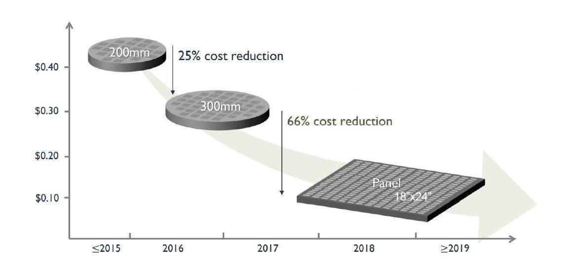
Panel-Level Packaging technology, especially Fan-Out Panel-Level Packaging (FO-PLP), is seen as the key to boosting AI chip production. Compared to traditional Fan-Out Wafer-Level Packaging (FOWLP), FO-PLP uses larger square substrates with an area utilization rate of over 95%, significantly increasing packaging efficiency.
TSMC is currently testing a rectangular substrate measuring 510mm by 515mm, which has more than four times the usable area of a traditional 12-inch circular wafer. This technological transformation is expected to significantly increase the output of AI chips, easing the pressure on the capacity of the current CoWoS (Chip on Wafer on Substrate) packaging technology.
Samsung: Early Explorer
However, in this race for packaging technology, Samsung Electronics appears to have taken the lead. As early as 2015, Samsung began advancing the development of FO-PLP technology and completed a strategic acquisition of the PLP business in 2019. The Tensor G2 chip in Google's Pixel 7 series, manufactured based on Samsung's 5nm process node, was packaged using FO-PLP technology for the first time in a mobile SoC, indicating that Samsung has had the mass production capability of FO-PLP since 2023.

Challenges and Opportunities of Panel-Level Packaging
Despite the obvious advantages of FO-PLP technology, it also faces several challenges in practical application. The first is the standardization of substrate materials and sizes, as well as the limitations of line width technical specifications. These technical difficulties require further innovation and breakthroughs to meet the design needs of high-performance chips.
Furthermore, the promotion of FO-PLP technology also requires the collaborative efforts of the entire industry chain, including material suppliers, equipment manufacturers, and packaging and testing companies. Only through the joint efforts of the entire industry can FO-PLP technology achieve large-scale production, reduce costs, and increase capacity.
Layout of Domestic and Foreign Manufacturers
In addition to TSMC and Samsung, many domestic and foreign manufacturers are actively deploying FO-PLP technology. For example, South Korea's Nepes has achieved mass production of a 600mm by 600mm square panel solution, and domestic companies such as FUTIAN FENG Microelectronics and YICHENG Technology are also researching and developing related technologies. In addition, panel manufacturers such as Innolux are also activating old production lines by converting them to high-value FOPLP semiconductor packaging production lines.

Conclusion
Panel-Level Packaging technology, especially FO-PLP, offers new possibilities for increasing the production capacity of AI chips. Although there are still technical challenges and issues of industrial collaboration, with the continuous maturation of technology and the expansion of the market, FO-PLP is expected to become another powerful force in the advanced packaging market. For chip manufacturers like TSMC and Samsung, whoever can make a breakthrough in this field may gain the upper hand in the future semiconductor competition.
Recommended Models
● The EP2C20F256I8N is a programmable gate array (FPGA) chip produced by Xilinx. It has a wealth of logical units, storage resources and I/O ports for complex digital signal processing and system-level integration. Manufactured with advanced process technology, it provides high performance computing power while maintaining low power consumption. Widely used in communication infrastructure, industrial control, automotive electronics, consumer electronics and other fields.
● The IR1167BSPBF is an intelligent secondary side drive integrated circuit (IC) manufactured by Infineon Technologies for driving N-channel power MOSFETs used as synchronous rectifiers in isolated flyback converters. Designed to control one or more N-MOSFETs in parallel, it uses 200V proprietary IC technology, operates at a maximum frequency of 500kHz, and is capable of delivering peak turn-off drive currents up to 7A. It is suitable for LCD and PDP TVS, telecom SMPS, AC-DC adapters, ATX SMPS, server SMPS and other application scenarios.
● The TMS320LF2406APZA is a digital signal processor (DSP) manufactured by Texas Instruments (TI). With processing speeds of up to 40MHz and 32KB of flash memory, it supports a variety of peripheral interfaces, including controller Local Area Network (CAN), serial communication interface (SCI), and phase-locked loop (PLL) -based clock generation. Widely used in automation and process control, motor drive and control and other fields. It is suitable for applications that require high-performance computing and precise control, such as industrial automation, power systems, automotive electronics, etc.


